 2022-11-16
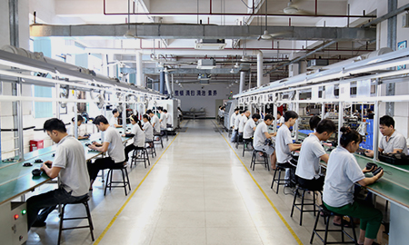
Generally speaking, the conventional surface treatment method widely used by chip processing factories in the process of pcb production design is OSP gold-plating immersion gold tin spraying. We can produce pcbs in terms of cost, solderability, wear resistance, oxidation resistance and chip production. The manufacturing process of the circuit board is different, and the drilling and circuit modification of the pcb circuit board have their own advantages and disadvantages. OSP process: This is low cost for smt chip processing plants, and the conductivity and flatness of pcb products are relatively high. Good, but poor oxidation resistance, not conducive to preservation.
The drilling hole of the pcb board is usually 0.1mm, and the HOZ copper thick line width compensation is 0.025mm. Considering that it is easy to be oxidized and contaminated with dust, the OSP process should be completed after molding and cleaning. When the size of a single piece is less than 80MM, it must be considered to be delivered in the form of connected pieces.
Electroplated nickel gold process: good oxidation resistance and wear resistance. When used for plugs or contacts, the thickness of the gold layer is greater than or equal to 1.3um. The thickness of the gold layer used for PCBA welding is usually 0.05-0.1um, but it is relatively solderable. Treasure or sex. Drilling compensation is performed at 0.1mm, and line width is not compensated. Note that when the copper thickness exceeds 1OZ to make a gold plate, the copper layer under the surface gold layer will easily cause excessive etching and collapse, resulting in solderability problems.
During the SMT process, the pcb factory needs current assistance for the gold plating of the pcb board. The gold plating process is designed before etching, and the complete surface treatment also plays a role in corrosion resistance. After etching, the process of removing corrosion resistance is reduced. The reason why the line width is not compensated.
PCB circuit board electroless nickel plating gold (immersion gold) process: good oxidation resistance, good toughness, flat coating is widely used in smt patch pcb board, drilling compensation is 0.15mm, HOZ copper thickness compensation is 0.025mm, because immersion The gold process is designed after the solder mask, so you need to use corrosion protection before etching, and you need to remove the corrosion resistance after etching, so the line width compensation is more board than gold plating, so after the solder mask, most lines have solder mask. Covering does not require immersion gold. Compared with large-area copper-clad laminates, the amount of gold salt consumed by immersion gold boards is significantly lower than that of gold-plated boards.
 Return


Address:The third, fourth and sixth floors of Building B, Zhonggaocheng Innovation Industrial Park, No. 10 Xinju Road, Shangjiao Village, Chang'an Town, Dongguan City
Landline:0769-81027015
Mr. Luo:15899912508

Fax:0769-81027025
 Follow WeChat public account
粤ICP备18111863号 Copyright © 2018Dong Guan Junze Electronic Technology Co.,Ltd all rights reserved


 CN
CN CN
CN