 2022-11-15
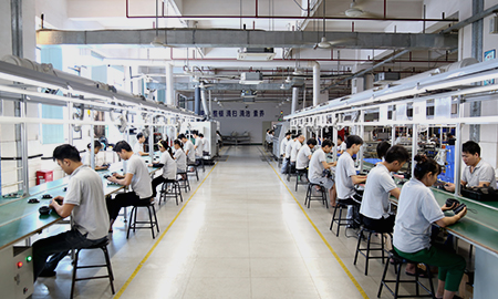
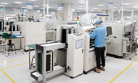
Generally, everyone knows the PCB multilayer board of the pcb factory. Refers to a PCB with one double-sided inner layer, two single-sided outer layers, or two double-sided inner layers and two single-sided outer layers. The circuit board is alternated by a positioning system and an insulating glue material, and the pcb board manufacturer needs to connect the pcb printed circuit board according to the conductive pattern according to the design requirements when designing the pcb board, also known as a pcb multi-layer circuit board. The seed board is a PCB multilayer board with better performance, which is inseparable from the careful design of the smt patch factory.
1. Determination of the shape, size and number of layers of the pcb board
1) Any pcb printed board has problems with other structural parts. Therefore, the shape and size of the printed circuit board must be determined according to the structure of the product. However, from the perspective of pcb chip processing and production technology, it should be as simple as possible, generally a rectangle with a small difference in aspect ratio, which is convenient for assembly, improves production efficiency, and reduces labor costs.
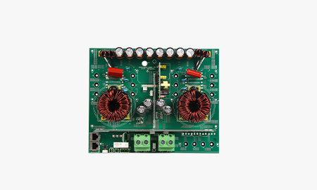
2) In terms of the number of pcb layers, it must be determined according to the requirements of the circuit performance, the size of the pcb board and the density of the circuit. For pcb multilayer printed boards, four-layer pcb and six-layer pcb are the most widely used. Taking a four-layer PCB as an example, there are two layers of wire (component side and soldering side), power layer and ground layer.
3) The number of layers of the pcb multilayer board should be kept symmetrical, and it is better to have a uniform copper layer, that is, four layers, six layers, eight layers, etc. Due to the asymmetry of the stack, the surface of the pcb circuit board is prone to warping, especially the pcb multilayer board mounted on the surface of the pcb board, which should be paid more attention to.
2. The position and direction of components on the pcb circuit board
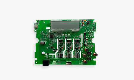
1) The position and placement direction of pcb components must first be considered from the circuit principle of the pcb circuit board to cater to the trend of the circuit. Whether the placement is reasonable will directly affect the performance of the PCB circuit board, especially for high-frequency analog circuits, which have stricter requirements on the location and placement of devices.
2) The reasonable layout of components on the pcb board, in a sense, indicates the success of pcb circuit board design. Therefore, pcb board manufacturers start to arrange the layout of the printed board when designing the pcb board. When determining the overall layout, they should conduct a detailed analysis of the pcb circuit principle, first determine special components (such as large ICs, high-power tubes, signal sources, etc.), Then arrange other components to avoid factors that may cause interference.
3) Another aspect here is that the chip processing factory should consider the overall structure of the printed board when designing the pcb circuit board, so as to avoid uneven arrangement of components on the pcb circuit board and garbled characters. This situation not only affects the appearance of the PCB circuit board, but also brings a lot of inconvenience to the assembly and maintenance work of the PCB factory.
 Return


Address:The third, fourth and sixth floors of Building B, Zhonggaocheng Innovation Industrial Park, No. 10 Xinju Road, Shangjiao Village, Chang'an Town, Dongguan City
Landline:0769-81027015
Mr. Luo:15899912508

Fax:0769-81027025
 Follow WeChat public account
粤ICP备18111863号 Copyright © 2018Dong Guan Junze Electronic Technology Co.,Ltd all rights reserved


 CN
CN CN
CN